1. What is UV lithography?
2. Working Principle of UV lithography
3. 2 common UV sources: mercury lamps and excimer lasers
4. What UV detector is recommended?
1. What is UV lithography?
UV lithography is a semiconductor manufacturing process used to create fine patterns and circuit structures on silicon wafers or other semiconductor substrates. This technique involves exposing a photoresist layer to ultraviolet light (UV), which is passed through a photomask containing intricate patterns. The exposed areas of the photoresist are then developed through chemical etching or other processing steps to transfer the pattern onto the substrate, thereby forming the structure of circuits or devices.
UV lithography is a critical step in modern semiconductor processes, with its resolution and accuracy directly impacting the performance and functionality of chips. As technology advances, UV lithography continues to evolve to meet the demands for higher resolutions and more complex circuit structures.
2. Working Principle of UV lithography
Ultraviolet lithography and exposure are core technologies in the semiconductor industry for producing various high-end chips and microcircuit structures. During the ultraviolet lithography process, UV light emitted by a light source passes through tiny lenses or gratings on a mask and is projected onto a photoresist layer, forming the desired micro-patterns.
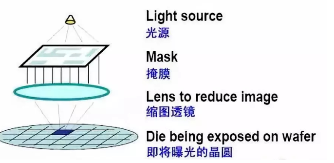
Figure1-light source
Traditionally, high-power mercury lamps and newer UVLED technologies have been used as UV sources in lithography equipment. UVLEDs offer unique technological and cost advantages, providing stable and high-power UV radiation over long periods, making them an ideal solution for semiconductor manufacturing. Many lithography applications rely on broad-spectrum exposure including wavelengths such as i-line, h-line, and g-line (365/405/435 nm).
3. 2 common UV sources: mercury lamps and excimer lasers
The intensity spectrum of a high-intensity mercury lamp is depicted in the figure. Depending on the wavelength chosen as the light source for lithography machines, they are referred to as G-line, H-line, I-line, or DUV. Longer wavelengths correspond to lower process capabilities and larger minimum feature sizes, indicating a more outdated technology. Therefore, in the nanometer era, sources usually contain 248nm KrF excimer lasers or 193nm ArF lasers.
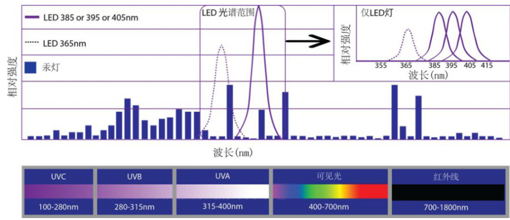
Figure2-mercury lamps and excimer lasers
Regarding the UV radiation intensity, which is crucial for production efficiency, sources like 248nm KrF excimer lasers are noted for their relatively low intensity, necessitating longer exposure times and reducing output per unit time. Hence, precise monitoring of UV lamp wavelength and intensity is essential in exposure equipment to avoid significant errors that could directly impact chip quality. For this purpose, in exposure equipment, high-radiation UV detectors are often required to real-time monitor UV lamp conditions.
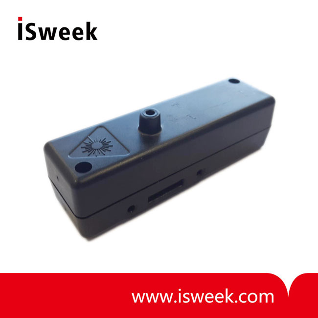
4. What UV detector is recommended?
ISWEEK recommends a high-radiation UV detector, the UV-Cure from Sglux in Germany. The UV-Cure sensor is designed for high UV irradiance (ranging from 20mW/cm² to 20W/cm²), operating at moderate temperatures (<80°C). It is typically used in UV curing systems with LEDs or medium-pressure lamps, offering configurable parameters such as signal output type, measurement range, and spectral response.
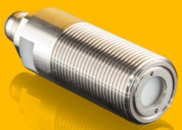
Figure3-UV-Cure sensors
UV-Cure sensors are available with analog outputs (4-20mA, 0-5V, or 10V) as well as digital communication options like USB, CAN bus, and MOD bus. Special variants of UV-Cure are also available, capable of operating at temperatures up to 170°C.
In summary, advancements in UV light sources and precise monitoring technologies like UV-Cure detectors are crucial for ensuring high-quality semiconductor manufacturing processes.